
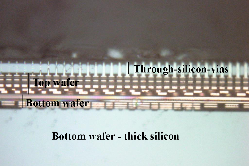
Cross-section of an early prototype of a vertically integrated sensor. The spacing of the through-silicon-vias is 4 microns. One of the challenges of constructing vertically integrated chips is aligning the layers. The bond between wafers is aligned to be about 2 microns. Recent runs have improved this to the sub-micron accuracy. Image: Donna Hicks, Fermilab