
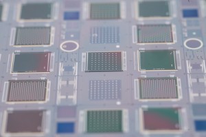
Fermilab’s vertically stacked chips bonded onto sensor wafers. Photo Credit: Reidar Hahn
In 2006, Fermilab’s Particle Physics Division teamed up with MIT’s Lincoln Labs to start work on the first iteration of a new kind chip for the proposed International Linear Collider’s vertex detector. A new way to slim down chips was emerging in the semiconductor industry, one that could potentially make it easier to measure the properties of incoming particles. Eight years and several iterations later, the chip is now close to being complete, and the ILC vertex detector is another step closer to being an engineering reality.
In old-fashioned circuit boards, components are arranged side by side on a flat surface. An electrical signal has to travel a long distance to reach the processor, and generates excess electrical noise in the process, reducing the clarity of the output. To solve this problem, the semiconductor industry started vertically stacking wafer-like silicon layers — each thinner than a human hair—and bonding them together chemically. The stacked arrangement is called a 3-D integrated circuit.
A 3-D arrangement is especially useful for the ILC vertex detector, where the chip and its associated sensor need to be as thin as practicable so as not to disrupt the path of the incoming particles too much and interfere with their properties. Furthermore, the circuitry needs to make do with limited power and still manage to capture a particle’s position, time stamp of arrival and charge at a good resolution.
Lincoln Labs and Fermilab collaborated to build this kind of a chip. The first iteration, VIP I – or vertically integrated pixel chip – was assembled in Lincoln Labs with three layers stacked together. The two labs went on to design a successor, VIP II-a.
“When we originally started working on it, our goals were pretty ambitious,” said Ron Lipton of Fermilab’s Particle Physics Division who worked on detector R&D for the ILC and worked with the engineers designing the chip. “But it was clear that if you wanted to really make progress, you had to have commercial technology.”
At this stage Tezzaron, based in Naperville, Illinois, and Ziptronix of Morrisville, North Carolina, were brought in to help develop VIP II-b, in which each wafer had a 192-by-192-pixel arrangement and greater resolution than its predecessors.
Tezzaron had created a working 3-D prototype in 2004 connecting two wafers with tungsten contacts embedded in the silicon, and Ziptronix had found a way to get rid of the 50-micron- thick solder bumps being used industrially to connect each pixel on a chip surface to the sensor. Ziptronix engineers had replaced the bumps with metal cylinders only 5 microns in diameter and 1 micron high embedded in a glass insulator, decreasing the distance between pixel and sensor by a factor greater than 10. These advances were integrated into the latest iteration of the VIP.
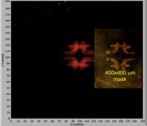
Tungsten mask of the Fermilab logo rendered using the VIP II-b chip. Photo Credit: Ron Lipton
So far VIP II-b has been tested qualitatively. A mask of the Fermilab logo made of tungsten, 400 microns thick, was pressed against the chip and bombarded with a radioactive source, and the chip was able to reproduce a readout of the pattern at a high resolution with relatively low noise. The result showcases the device’s abilities and serves as testament that the basic circuitry works.
Next up is detecting an actual particle beam. A collaboration between Argonne National Laboratory, Brown University and Fermilab to optimize the chip quantitatively for such a setup is under way.
“We have all of the pieces necessary to build a functional prototype for the vertex detector,” Lipton said. “The next step will depend on how the ILC project proceeds.”
Recent Comments