 |
|||||||||||
|
|||||||||||
|
|||||||||||
|
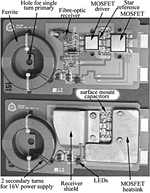
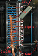
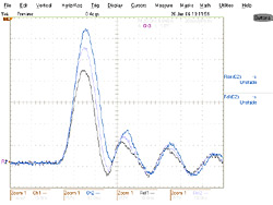
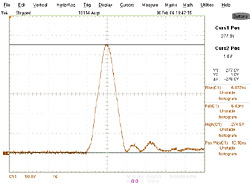
The rise and fall times of the pulses in the injection kickers influence the minimum circumference of the damping rings in the International Linear Collider. The Baseline Configuration Document features 6 km rings which will require pulsers to feed 50 ohm stripline kickers. The 5 kV (kilovolt) pulses must have 6 ns (nanosecond) rise and fall times, and a total duration of approximately 14 ns. Operating in a burst mode, every 5 seconds the kicker will have a 3 MHz (megahertz) burst that lasts 1 ms (millisecond). The combination of the electric component from the 5 kV voltage pulse and the magnetic component from the accompanying 100 A (amp) current pulse will deflect the electron and positron beams. The temporal specification of the kicker pulse presents a challenge to the existing generation of pulser technology. Previously, the TRIUMF kicker group designed and built a kicker for the Paul Scherrer Institute (PSI) with deflection voltages up to 25 kV at 75 kHz (kilohertz) continuous wave and with 40 ns rise and fall times. Each of the 4 modulators in the PSI kicker consists of two stacks of 17 series 1 kV Field Effect Transistors (FET): the present design of the MOSFET card (fig 1) allows a FET to collapse almost 1 kV in approximately 3 ns. This does not translate however to fast switching times for a stack of FETs when combined in the conventional manner. The TRIUMF kicker group is now developing a new modulator circuit concept for an ILC kicker. The group conducted proof of principal tests using the PSI kicker prototype as a test bed and a setup using components on hand (Fig 2). The final design will use two parallel 100 ohm drivers combined to provide a 50 ohm kicker. The test circuit, which is a single 100 ohm driver, has been used to generate 5 kV pulses, with 6 ns rise and fall times, into a high-power 100 ohm load at 1 kHz. The post-pulse ringing in Fig 3 is attributable to impedance mis-matches. The total width of the pulse at the base was 20 ns compared with the required14 ns. Tests with .5 kV pulses into a low-power load with smaller inductance show much reduced post-pulse noise (Fig.4). As a result of these encouraging tests, the kicker group will make a series of design improvements to meet the ILC kicker specifications. The 3 MHz burst mode requires fast charging circuits, and the impedance matching needs to be more precise than in the prototype. Reduced inductance will lead to shorter pulse lengths and shorter rise and fall times. New lower inductance FET cards have been designed, and the stack configuration is also being modified with the goal of reducing the inductance to approximately 620 nH (nano-Henry) or less. In addition it is planned to eliminate the fibre optic triggering used on the present FET cards. -- Shane Koscielniak, TRIUMF |
|||||||||||
| © International Linear Collider |


