 |
 |
|||||||||||||
|
|||||||||||||
|
|||||||||||||
|
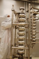
Turkey, stuffing and pumpkin pie – all things you might appreciate on Thanksgiving. ILC scientists in the United States had something extra to be thankful for this year. On 21 November, the day before the Thanksgiving holiday in the US, a superconducting cavity manufactured by Advanced Energy Systems in Medford, NY, reached a high gradient of 32.6 megavolts per metre (MV/m) at Jefferson Laboratory. This is the first US-built ILC nine-cell cavity to reach a gradient close to the ILC specification, said Rongli Geng, the lead scientist at JLab on the nine-cell high-gradient cavity processing R&D. JLab scientists are hopeful that the cavity, dubbed AES2, will reach an even higher gradient after further processing.
The target gradient for each ILC cavity is 35 MV/m, and ILC scientists around the world are working toward this goal. The AES2 gradient is significant because it demonstrates the increasing capabilities of US cavity vendors. In comparison to manufacturers in Europe and Asia, US vendors are considered new to the game and reaching a gradient of 32.6 MV/m shows significant progress. “This is a very encouraging result,” said Fermilab's Shekhar Mishra. “It shows that a US vendor can produce an ILC-quality cavity. JLab is doing an excellent job in advancing the high gradient cavity processing R&D.” Fermilab purchased the first four US manufactured ILC nine-cell cavities, and JLab started processing and testing them in April 2007. Using the facilities at their Superconducting Radio-Frequency Institute, JLab performed the current standard ILC electropolishing process along with the lab's developed final cleaning and assembly steps. First, the cavity undergoes a heavy initial electropolishing to remove 150 microns of the damaged layer. Then, the cavity bakes for approximately 10 hours at a high temperature of 600 degrees Celsius to remove hydrogen from the niobium material. After some tuning for field flatness, basically calibrating to maintain a flat electromagnetic field, the cavity receives another light electropolishing. The second round of electropolishing removes the contaminated layer of material that results from the baking process. Next the cavity receives ultrasonic cleaning with a detergent solution - a JLab twist on the ILC standard recipe. Finally, after high pressure water rinsing and clean room assembly, the cavity pumps down to vacuum. Then, after another round of baking at a lower temperature of 120 degrees Celsius to address the slope in the Quality factor, the cavity is ready for testing. “It is very tempting to improve on the process as you go along, but we need to be consistent and do it the same way every time,” said Bob Rimmer, who is in charge of JLab's SRF Institute. After the AES2 cavity went through this entire process, it initially reached a gradient of 19.6 MV/m. JLab wasn't ready to give up though and electropolished the cavity again. Geng explained that the gradient of AES2 increased as they removed surface material. After the fourth light electropolishing, AES2 finally reached its record gradient of 32.6 MV/m - a vast improvement from the initial results. Scientists suspect that the niobium material used for this cavity may have had defects, which is why the removal of surface material would improve its performance. “If this is true, further performance improvement is anticipated,” said Geng. “We will electropolish and test the cavity again.” In addition to AES2, JLab is testing the AES4 cavity now. Initial tests indicate that it too will have a high gradient. “They haven't reached their quench limits yet,” said Rimmer. Both Rimmer and Geng agree that the positive results would not have been possible without the dedication and successful teamwork of many colleagues, including JLab's Curtis Crawford, Byron Golden, Pete Kushnick, Jeff Saunders, Kurt Macha and Fermilab's Damon Bice. -- Elizabeth Clements |
|||||||||||||
| © International Linear Collider |
