 |
 |
|||||||||||||
|
|||||||||||||
|
|||||||||||||
|
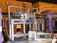
The sixth meeting of the Silicon tracking for the Linear Collider R&D Collaboration (SiLC) took place at the University degli Studi in Turin from 18 to 20 December 2007. The three-day meeting was attended by about 50 people and covered all the main topics of interest for this R&D. The SiLC generic R&D was launched in 2002. Its aim is to develop the next generation of the large silicon tracking systems. Several SiLC partners are members of the European Union-funded EUDET project. One of the crucial SiLC R&D objectives is the development of new sensors including new microstrip sensors and pixels. In both cases, we also anticipate the applications of the three-dimension integration technologies to be one of our future goals. Another major goal is the deep sub micron (DSM) front-end (FEE) and readout electronics, with a direct connection of FEE chips on the detector. They are developed in collaboration with industry, namely the Japanese firm Hamamatsu Photonics (HPK). During the meeting, we reviewed the mechanical issues principally related to the high performances required for spatial resolution and lowering the material budget, such as cooling, alignment and new materials. Why reduce the material budget? Actually this is a crucial requirement since each atom of matter on a particle trajectory is likely to disturb it and thus to degrade the measurement. This goal is reflected in all the aspects of the SiLC R&D and will be the major achievement for us if we succeed. We use the semi-conductor technology for both detection devices and their associated front-end and readout electronics. It will allow us to build a fully integrated system where electronics and detector are closely related. At the same time, it will push further the impressive progress in this challenging and promising technological field with interesting outcomes in several applied domains. The lab test bench, test beams and the simulations are main essential R&D tools to characterise our sensors. Last year, the main outcomes were the development of a SiLC simulation task force which had a dedicated parallel session during this meeting. Same for the test beam which was led at CERN in October 2007. The result of these tests was the successful characterisation of new, large, thinner and smaller pitch microstrip sensors produced by HPK, according to our requests, mounted onto modules read out with the new front-end and digitised readout chips developed by this R&D project in a 130-nanometre CMOS technology (Complementary Metal-Oxide Semiconductor). The meeting was an opportunity to emphasise the synergy on silicon trackers between the Large Hadron Collider (LHC) and its upgrade the Super LHC, the SuperB factories (at Frascati and KEK) and the ILC. The benefit of working closely together was clearly demonstrated and interesting presentations were given by representatives from these various facilities. Actually, we can summarise it in giving another explanation for the SiLC acronym: Silicon tracking for Large Colliders. Last but not least, we sampled the excellent Piemontese gastronomy in great detail with the succulent dinner and wines; it reinforced our determination in pursuing our challenging and promising R&D! -- Diego Gamba and Aurore Savoy-Navarro See also the meeting website |
|||||||||||||
| © International Linear Collider |

