 |
 |
|||||||||||||
|
|||||||||||||
|
|||||||||||||
|
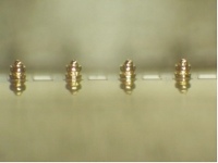
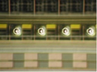
Nearly every one of the myriad complex components of the International Linear Collider pushes the limits of today's technology, and for the ILC to succeed, each one of them has to work as designed. Researchers at the University of California, Davis (US) are concentrating on the interconnects – the connections between arrays of electronic circuit elements – in the ILC's proposed Silicon Detector Design Study (SiD) concept detector. The group is applying new technologies and advanced materials to improve the performance, efficiency, ease of assembly and robustness of these critical detector components. In 2005, UC Davis's recognised expertise in interconnect technologies led them to join the silicon-tungsten, or SiW, group, which includes researchers from SLAC National Accelerator Laboratory, the University of Oregon, and Brookhaven National Laboratory within the SiD collaboration. “We have been involved with indium bump-bonding since the early 1990s, and we did the prototypes for the large hadron collider's CMS forward pixel detectors among other projects,” said UC Davis physicist Richard Lander. Bump bonding is the use of microscopic dots of conducting material, such as indium or solder, to connect electronic circuit elements. Bump bonds are essential in connecting detector components in the pathway that leads from a particle collision, to a sensor, to a silicon chip, to a readout device, to data acquisition electronics, to a researcher's computer. Technicians align the bumps on one component – a silicon sensor, for example – to the bumps or metal pads on another – say a microchip – and apply heat and pressure to join the two elements. In the SiD detector, particles showering out from a collision in the heart of the detector pass through layers of silicon sensors sandwiched between layers of tungsten. When particles interact with the silicon, the sensor conveys the signal to a silicon chip at its centre. The UC Davis group is refining a method that uses flex cable, a wide cable with copper traces embedded in a plastic substrate, to connect a series of these chips and convey their signals to readout devices at the detector's perimeter. It's a precision process, fraught with technical challenges, among them dealing with the two-metre lengths of flex cable that the detector will require.
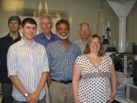
“Silicon-tungsten calorimetry is a great idea,” said UC Davis physicist Mani Tripathi, “but to make this happen, these interconnect technologies need to be perfected.” New materials also hold promise for advancing interconnect technology, and the UC Davis group is at the forefront of efforts to develop their potential. The group is currently investigating the use of gold in bump bonding. Although it has its own challenges, gold's resistance to oxidation gives it an advantage over other materials traditionally used in bump-bonding. Currently gold stud bumps are attached to the substrate with conductive epoxy, but efforts are underway to use stud bumps on both chip and substrate. Anisotropic conductive film (ACF), a material consisting of nickel fibers embedded in thermoplastic material, may offer an alternative to bump bonding. The fibers have an oxide coating in the direction transverse to their axis and hence act as insulators in that direction while acting as conductors along their axis. When sandwiched between two sets of electronic components, compressed, and heated to set the thermoplastic material, the ACF film makes the connection. Ultimately researchers plan to use the material to connect 16 sensor chips along a two-metre length of flex cable leading to a readout device. Besides physicists Lander and Tripathi, the UC Davis interconnect group comprises Brill Holbrook, an electronics engineer, Mike Woods, a graduate student, and technicians Tiffany Landry and Mike Irving. The UC Davis group hopes its pioneering work will have industrial applications beyond the field of particle physics. The university has strong working relationships, with industrial firms active in technologies closely related to HEP, including Shared Resources in San Jose, California; Palomar Technologies in Carlsbad, California; Aspen Technologies in Colorado Springs, Colorado; and Flex Circuit Technologies in Plymouth, Minnesota. “We really do hope to give useful technology back to industry for their use,” said Tripathi. “We are always trying to partner with companies and hopefully they can take our research results and expand their technology.” The university hopes to have key elements of their interconnect technology research completed by December 2009, an ambitious plan that is integral to the construction of a 30-layer prototype of the SiW calorimeter. “Our goal is to complete the assembly and test it in a beam during 2010,” said Tripathi. -- Andre Sulluchuco |
|||||||||||||
| © International Linear Collider | |||||||||||||


