 |
 |
|||||||||||||
|
|||||||||||||
|
|||||||||||||
|
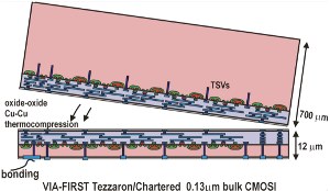
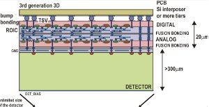
The International Linear Collider had more than a dozen circuit pixel-detector technologies to choose from for their vertex detectors. Now, they can choose from many more design options thanks to a ground-breaking partnership among national laboratories, universities and industry. This partnership of 17 European universities and US national laboratories with industry to explore the applicability of the 3-D silicon technology for particle physics could lead to an increase in detector precision as well as improved technology for medical applications including X-ray machines and surgical devices. This 3-D silicon technology project was formed in early 2006 as part of Fermilab's initiative to improve resolution and processing speed of detectors to meet the demanding ILC detector requirements. In 3-D silicon technology, thinned silicon layers are vertically bonded together and electrically connected to form one integrated unit. They can, in turn, provide more data storage space, can consume less energy, and process information quicker than traditional flat circuits. The 3-D project has allowed universities and industry communities to address certain challenges of the technology in their efforts to design new forms of pixel detectors with improved performance. Historically, universities, laboratories and industries have not joined in the design process at the same time or this early in the approval process. “This is the first time a high-energy physics project is working together with a commercial company in this way,” said Marcel Demarteau, a Fermilab scientist specialising in detector design. Fermilab is partnering with Tezzaron Semiconductor, a technology company based in the Chicago suburbs, to build each of the 15 submitted designs. The company will work with a silicon foundry in Singapore to manufacture the circuit prototypes, and Fermilab will receive the final assembled circuit pieces within a month. This collaboration may eventually allow scientists to explore many additional options for ILC detectors. “The ILC is a driving force in the search for new transformational technologies,” said Demarteau. For the last few weeks, the silicon detector team at Fermilab has been reviewing pixel circuit sensor designs received from the 17 collaborating universities in Europe. “We are now determining the design applications that will work best with the technology,” said Ray Yarema, a senior engineer at Fermilab. Laboratories and universities from France to Italy to Germany seized on the chance to work together in early 2007. “It's mostly the European researchers who work on projects like monolithic active pixel sensors or MAPS,” said Grzegorz Deptuch, an engineer at Fermilab. This collaboration gave them the opportunity to improve on MAPS designs, which had some limits on performance, and to bring about better designs and circuits. “This sharing of ideas among academia and industry is really thanks to the ILC. This has clearly benefited the community at large,” said Demarteau. This project became a learning process for both researchers and industry involved since the project and design needs are very specific. This autumn, the 3-D silicon technology project will hold a meeting where users and designers will evaluate all the contributed circuits, share design experiences, and test the characteristics of those designs. “We strongly benefited from industry pushing this technology,” said Demarteau, “and we were able to use this in the early development stages.” -- Andre Sulluchuco |
|||||||||||||
| © International Linear Collider |

