
Inside your pocket-sized mobile device, there likely sits a Lego-brick-sized camera inside of which lies a thumbnail-sized sensor. The sensor, sliver though it is, is on its way to being smaller.
ILC researchers have been developing more compact pixel sensors, similar to those in cell-phone cameras, for detecting particle showers. The sensor’s diminished size is thanks to a semiconductor innovation called vertical integration, more familiarly known as 3-D sensor technology.
“The 3-D technique lets you build the sensor up rather than across,” said Fermilab’s Ron Lipton, who works on detector R&D for the ILC. Like skyscrapers, these newer sensors create and make use of vertically available real estate, enabling tighter connections between components and freeing up the horizontal space for still more sensors.
Or as Lipton put it, “It makes a horizontal sandwich.”
Standard chip components are arranged roughly side-by-side on a single plane. The central processing unit is situated next to the memory, and signals from millions of memory cells travel along horizontal paths to get to the processor.
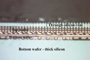
Cross-section of an early prototype of a vertically integrated sensor. The spacing of the through-silicon-vias is 4 microns. One of the challenges of constructing vertically integrated chips is aligning the layers. The bond between wafers is aligned to be about 2 microns. Recent runs have improved this to the sub-micron accuracy. Image: Donna Hicks, Fermilab
By layering the device’s components on top of each other rather than laying them next to each other, researchers are able to reduce the chip’s overall size.
What the sensor loses in size, it gains in data quality and transmission. Shorter, more direct circuitry between pixel and processor allows for higher bandwidths, enabling information to move faster. It also saves power that would otherwise be wasted on longer-than-necessary electrical pathways and resistive elements. The layering technique makes room for more pixels and memory, yielding higher-quality and higher-resolution data.
“It allows you to save on a number of levels,” Lipton said.
Around 2006 ILC scientists learned about 3-D technology and consulted with MIT-Lincoln Labs in Lexington, Massachusetts, US, to develop lean, efficient and high-quality 3-D pixel sensor prototypes for the ILC’s detectors.
The first thing the chip needed was a good slimming down.
Circuitry only occupies the seven-or-so topmost microns of the sensor’s processing chip. The rest of the chip’s mass simply gives you a way to handle it. It’s nonessential.
“The top few microns is where all the action is, where all the brain power is,” said Argonne National Laboratory’s Marcel Demarteau, chair and convener of the ILC Common Task Group. “For us, the rest is just redundant. If you can get rid of that mass, it’s better.”
For 3-D sensor technology, the bulk of the processing chip is sanded down to close the roughly seven-micron-thick silicon wafer housing the circuit.
In the 3-D integrated configuration, the sensor, comprising millions of pixels arranged in a grid, lies squarely beneath the processing chip. Between them are the electrical connections, which go from pixel (in the bottom layer) to processor (the top layer), and an agent to keep them aligned.
In its bulkier form, the processing chip is soldered to the sensor. Though solder bumps get the job done, serving as both glue and electrical connections between each pixel and the processor, they tend to be expensive to apply and, at roughly 100 microns, make the chip size larger than what ILC researchers wanted.
Faced with a now razor-thin processing chip that had lost its bulk, researchers needed a new way to connect the two slivery layers. They turned to oxide bonding, a technique that has been under development for about a decade, to glue them together. And rather than rely on solder bumps, the electrical connection between each pixel and the processor would be forged through microscopic tungsten pillars, called through-silicon-vias (TSVs). These pillars, which can be anywhere from 1.5 to 20 microns thick, would replace the solder bumps, boulders by comparison. The TSV emerges as a slender stem from each of the millions of pixels in the sensor and shoots up towards the processor ceiling. The base of the TSV is necessarily much smaller than the pixel from which it emerges, leaving as much of the pixel space as possible available for data collection.
The net effect of cutting mass and switching out larger parts is a sensor that is 10 times smaller in depth and in area – a useful improvement when you’re designing a detector.
“A lot of the pain in designing these detectors is finding out how you can fit the sensor with all its functionality in the geometry that’s available,” Lipton said. The sensors are designed for the innermost part of the detector, called the vertex detector, which immediately surrounds the particle collision site. Reduced in size, now thousands of these compact sensors could fit into their assigned space, about the size of a paper towel roll.
The semiconductor industry hasn’t yet developed 3-D technology to the state of the art. The design software infrastructure and development of industry standards need further work. Still, detector researchers believe it’s only a matter of time before vertically integrated sensors, crucial for the development of particle detection, are good enough that other fields of science may want to take advantage of them.
“There’s enormous potential for memory devices,” Demarteau said. One vertically integrated sensor could accomplish a prodigious amount of work for applications that rely on memory and pattern recognition, such as iris scans for security or biochips for medicine, by speeding up the process of mining billions of patterns. “Once you start talking about those possibilities, you open up whole new fields of science. The market is enormous for this technology,” he said.
ILC researchers are currently working with companies Tezzaron in Naperville, Illinois and Ziptronix in Morrisville, North Carolina to develop prototypes of the pixel sensor, which they expect will be ready around May.
Recent Comments