
2015: The first fully functional Belle II pixel module seen from the front and back side. The reflection shows the thin sensitive area with the perforated support frame.
Back in the early days of the new millennium when TESLA was not linked to electrically driven vehicles but the name of an ILC predecessor project, a small group of physicist and engineers from Bonn and Munich came together to discuss what they can do to face the challenges in future high-energy physics experiments. The goal was to determine the vertex – the place where the particles collide and interact – with the highest precision at maximum read-out speed. In the end they came up with the idea to use active pixel sensors operated in rolling shutter mode to minimise power consumption and material in the sensitive volume.
Feasibility studies were made and the development gained momentum, first prototypes were built, and with that the concept gained visibility. Scientists working on the Belle II detector at the SuperKEKB accelerator in Japan chose this technology for their vertex detector. The small group developed into the DEPFET Collaboration with institutes from all over Europe. DEPFET stands for “depleted p-channel field-effect transistor.” In the subsequent years the concept was brought to an engineered solution which was recently finalised with the construction of ‘Module-0’ – the first all-silicon module that could be used in the final Belle II experiment.

2003: First conceptual sketch for the all-silicon module comprising a thin sensitive area with active pixels and supported by a rigid frame carrying read-out and steering ASICs.
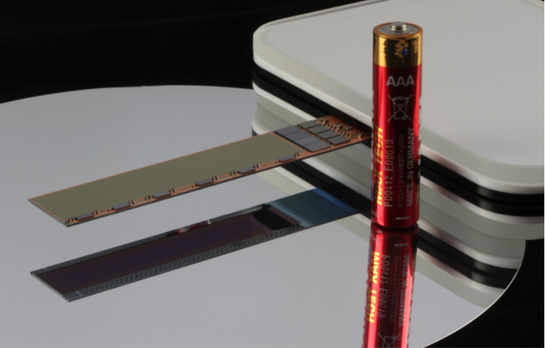
Made from silicon a thousand times more pure than conventional transistors or memory chips, the module integrates 200,000 DEPFET pixel cells on a surface area of eight square centimeters. It was invented at the Semiconductor Lab of the Max Planck Society (MPG HLL) and is fabricated here exclusively.
The DEPFET component enables the detection of photons – or, as in this case, of high-energy particles – with the utmost efficiency and precision. The fundamental process is very similar to the one in a conventional photo or video camera. However, the primary signal from individual photons or particles is very much smaller.
This is where the major advantage of the DEPFET comes into play: the tiny primary signal is amplified within the sensor itself. Thus the DEPFET is the sensor material and the first stage of amplification rolled into one. Arranging many DEPFETs in a matrix forms an image sensor with which a particle’s point of interaction can be precisely determined. In the present configuration for the Belle II experiment this can be done with an accuracy of around one-hundredth of a millimetre.
Control of the pixels in a matrix and ultra-fast processing of the DEPFET signals require additional electronics, which have been developed and produced in collaboration with University Bonn, University Heidelberg and KIT Karlsruhe. These electronics, in the form of application-specific integrated circuits (ASICs), are placed directly on the sensor substrate. The ASICs allow digitisation of signals from the pixel matrix, as well as lossless data compression, to transmit them off-module at the highest speed (50,000 frames per second).
With this, the DEPFET matrix becomes a very complex module with maximal integration density, which despite all its complexity is extremely thin and light, so that the measurement accuracy of particle tracks is not distorted by the sensor material itself.
The MPG HLL has developed a unique technology for this purpose that makes it possible to fabricate extremely thin and highly integrated sensor modules. In the fabrication process, the sensitive part of the module, the DEPFET matrix, is thinned by a customised etching technique to 75 micrometers, roughly the thickness of a human hair.
These bendable silicon films are supported by a monolithically integrated silicon frame, on which the readout and control electronics are mounted. The power supply and data lines run through a flexible ribbon cable, which is attached to the end of the module.
The MPG HLL technology makes it possible to arrange the thin DEPFET matrices in a cylindrical form, without any further support, around the interaction point of the experiment. With that, the highly precise measurement of particle tracks is becoming reality.
More information:
Recent Comments