
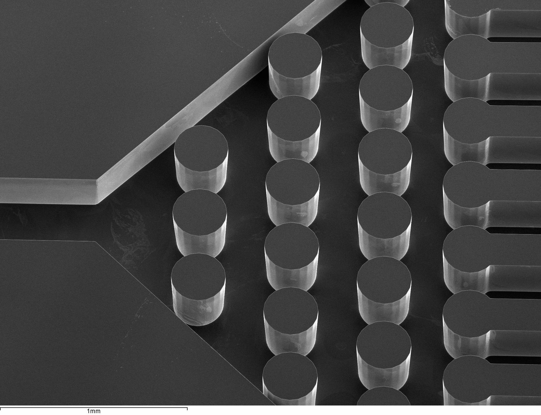
The micro-channels etched into the primary handle wafer before sealing the circuit with the second sensor wafer. Image: L. Andricek, MPG-HLL, Munich.
Riding the wave of progress in semi-conductor industry, pixel vertex detectors have improved their performance dramatically over the last decades. It is now possible to build ultra-thin devices with a spatial resolution of several microns, while maintaining a read-out speed and power- consumption that is adequate for lepton collider experiments such as the ILC.
Several groups are developing the next generation of detectors for e+e- colliders. The most well-known are the monolithic devices of the CMOS-family and the DEPFET active pixel detectors (the name stands for Depleted Field Effect Transistor). Both these technologies have reached maturity; MAPS and DEPFET vertex detectors are being constructed for use in collider experiments as we speak. Further progress is expected from HV-CMOS, 3D-integrated devices,
These new devices can discriminate signals of a few 100 electrons. This has allowed to reduce thickness of the sensors drastically, from the equivalent of nearly one millimetre of silicon to close to 100 microns. Getting rid of every gram of material that we can is key to achieving the resolution required by lepton collider experiments, as charged particle trajectories are affected by interactions with the detector material. The obsession with losing weight does not only extend to the active sensor, but to all parts of the detector system that get in the way of the particles.
At the heart of the detector for the ILC there is no room for bulky support structures or cooling systems. The DEPFET collaboration therefore integrates these functionalities in the detector design. In an R&D effort partly financed by the AIDA2020 project, Max Planck Society’s semiconductor lab in Munich MPG-HLL, the University of Bonn and IFIC in Valencia are developing a process to integrate the cooling circuit in the active silicon sensor. In industry, micro-channel cooling is used to cool, for instance, memories. In high-energy physics (HEP) experiments, LHCb, NA62 and ALICE use silicon cooling plates based on the principle. A monolithic integration of the cooling system in the same silicon wafer that acts as active detector material, however, has not yet been attempted.
The process starts off with two silicon wafers. The cooling manifold of arbitrary layout is etched (using DRIE etching) in a thick handling wafer. A photograph of part of one of the manifolds from first test production run is shown in Fig. 1. The circuit is sealed with the sensor wafer that is bonded on top of the handle wafer. All except the strictly necessary material can now be removed by combination of mechanical and chemical processes. The result is an ultra-thin self-supporting detector with a tiny cooling circuit hidden inside.
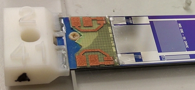
A mechanical sample with integrated cooling with the 3D-printed interface to commercial fittings. Image: M. A. Villarejo, IFIC Valencia
The connection of the tiny inlet and outlet – with a cross section of 350 x 400 mm² – to the main cooling circuit is possibly the biggest hurdle for the deployment of micro-channel cooling in high energy physics. State-of-the-art solutions, such as the soldered Kovar connectors used by LHCb, are too bulky for application at the heart of the experiment. The IFIC-Bonn-MPG groups have therefore opted for plastic connectors, such as those shown in Fig. 2. These complex structures can be fabricated quickly and at very low cost thanks to the advent of 3D-printing. The high precision of this process ensures that the cooling lines in connector and sensor self-align. The experience so far has been very positive; the first batch of assemblies has been built with 100% yield.
A number of prototypes have been tested at the thermo-mechanical laboratory at IFIC, with very encouraging results. A tiny trickle of cooling fluid (i.e. 1 l/h of water) is sufficient to remove up to several tens of watts from the sensor area. As the cooling liquid and the heat source are separated by only a few tens of microns of silicon, the temperature difference between coolant and the hottest spot on the sensor is minimal. The first structures have moreover been submitted to leak and pressure tests at CERN, where they are found to stand well over 100 bar (How did we find out? Though one of the most smashing experiences after all the careful handling of our prototypes…).
The success of this first exploratory study encourages us to further develop micro-channel cooling for HEP applications. It provides a good example of how advancing technology may help us to satisfy the ever more challenging specifications of collider experiments. The possibilities offered by ultra-precise silicon lithography and processing are well-known, but many opportunities remain to be exploited. And we are only just beginning to explore the vast potential of 3D stereo-lithography!
Further reading: L. Andricek, M. Boronat, I. Garcia Garcia, P. Gomis, C. Marinas, J. Ninkovic, M. Perello Rosello, M.A. Villarejo, M. Vos, Integrated cooling channels in position-sensitive silicon detec tors, arXiv:1604.08776, submitted to JINST (https://arxiv.org/abs/1604.08776)
Results are to be presented at the tracker mechanics forum in Bonn, the tracker/vertex detector session of the ECFA Linear Collider meeting in Santander and in the AIDA2020 annual meeting. AIDA2020 is funded by the EU H2020 framework programme under grant agreement.
Recent Comments