
A necklace of cheap metal with gold-flaked paint may look like solid gold finery, but eventually, the paint will peel, revealing a worthless trinket beneath.
But an accelerator cavity of inexpensive metal with a nice niobium coat, though less expensive than a solid niobium structure, could actually hold more value for a particle collider.
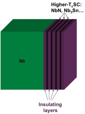
For multi-layer superconducting films, a bulk, one-micrometre layer of niobium is further coated with niobium-compound, nanometre-scale thin films. For accelerator cavities, this combination of superconducting layers could be applied to an aluminium or copper cavity and achieve acceptable magnetic fields. Image courtesy of Thomas Proslier.
Scientists at Argonne National Laboratory in the US are developing a method that uses atomic superconducting layers to evenly cover, like the perfect coat of paint, the insides of cavities. Since electric current flows only through the cavity wall’s innermost hundred nanometres, thin niobium-compound films could provide an alternative to pricier, solid niobium cavities.
“We’re trying both to make better superconductors and to make them more cheaply,” said James Norem, accelerator physicist in Argonne’s High Energy Physics Division.
Using atomic layer deposition (ALD), as the method is called, scientists line bulk metals with nanometres-thin superconducting films. In one cavity model, a copper or aluminium body would support a micrometre-thick niobium layer (an amount still considered to be in the bulk range). Niobium-compound thin films are grown over it.
Realising this model could save money on several fronts. For a project like the ILC, the savings could range in the hundreds of millions of dollars.
One reason is that aluminium and copper are cheaper than niobium. Also, cavities would not have to be kept as cold as 2 kelvin (the current target temperature for niobium cavities) to superconduct effectively, cutting refrigeration costs; the operating temperature depends on the niobium compound used. Films also eliminate the need for the usual extensive surface treatment of niobium cavities. And because niobium compound-coated cavities can achieve comparable or higher gradients than solid niobium ones, an accelerator would require far fewer of them.
But achieving those gradients depends on growing perfect, uniform layers. Researchers believe ALD can make that happen for accelerators.
“We’ve grown by far the best superconducting film ever with this technique,” said Argonne’s Thomas Proslier, who is leading the laboratory’s effort on ALD for cavity coating. So far Argonne researchers have tested the technique on various flat surfaces of aluminium, copper, niobium (niobium-compound films can enhance already-superconducting metals) and sapphire.
In one test, Proslier’s team was able to grow a niobium nitride thin film that could superconduct at 14.5 kelvin, a temperature almost two-thirds higher than pure niobium’s critical temperature of 9 K. They grew it on a flat substrate.
Coating flat surfaces is one thing. Evenly covering the undulating insides of an accelerator cavity is another beast altogether.
“You have to homogeneously coat the whole inside of the cavity, so the coating method can’t depend on line of sight,” Proslier said. “The strength of this technique is that it can coat arbitrarily complex-shaped objects.”
With ALD, thin films are formed from gases that react with the substrate metal in a way that its surface becomes saturated with the gaseous atoms. As many atoms that can be attracted to the metal will be. Once they are, there’s no room for any more to alight.
“Even if you wanted to, you couldn’t make more than one atomic layer at a time,” Proslier said.
The process ensures that only a single, superconducting stratum is deposited, one that settles as uniformly on curves and in crevices as it does on flat planes. As scientists like to say, the layer is conformal.
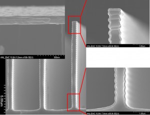
Atomic layer deposition results in a conformal thickness of material. The layer evenly and uniformly coats any surface geometry. Image courtesy of Thomas Proslier.
Different combinations of gases are used to build up the atomic layers, both superconducting and insulating, to get the desired multi-layer combination, which ends up being about 300 nanometres thick.
“The theory says that if you have a sandwich of superconducting and insulating layers, then you can get to higher fields than you would otherwise,” Norem said.
To optimise the multi-layer structure, they examine the various gases’ chemical compositions. They also look at the resulting layers’ crystallographic structure, superconducting properties, critical temperatures, densities and thicknesses.
“Right now we’re trying to grow the multi-layer with as good as properties as we can get out of it,” Proslier said. “We do everything we can to match the layers in the best ways possible.”
Alex Gurevich, a condensed matter physicist now at Old Dominion University in Virginia, developed the theoretical basis for the behavior of superconducting multi-layers. Michael Pellin, an Argonne Distinguished Fellow and former Materials Science Division director, along with Norem and Proslier, saw that multi-layer thin films could be applied to accelerator cavities.
The Argonne team has been researching the technique for cavities with funding from the Department of Energy since 2009.
By this summer, Argonne researchers hope to complete ALD tests on single-cell niobium cavities. From there, they will move on to copper cavities and other higher-critical temperature materials.
“We’ve been optimising niobium cavities for 20 years,” Norem said. “Now we’re starting to work with materials that are potentially superior.”
Recent Comments