
Superconducting radiofrequency power only runs skin-deep, and accelerator scientists have been taking advantage of the phenomenon’s surface-crawling tendencies with a view to making high-performing, low-cost accelerator cavities. The trick is to manipulate a metal’s top-most layer so that it conducts just like a thick slab of superconducting material.
Scientists at Jefferson Laboratory in the US are researching a deposition technique for applying thin niobium films to a metal’s surface. The approach, layer deposition via electron cyclotron resonance (ECR), allows them to fashion fine layers into something that could be mistaken for the tried-and-true superconductor standby, bulk niobium.
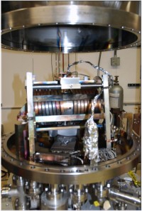
Vacuum chamber for energetic condensation via electron cyclotron resonance. The vacuum chamber is open to show the coil structure in the center. Niobium atoms are ionised inside the coil by electrons. The substrate on which the ions are deposited is positioned at one end of the coil. Image courtesy of Anne-Marie Valente-Feliciano.
“The top layers should effectively mimic bulk niobium performance,” said Anne-Marie Valente-Feliciano, scientist in the Process and Materials Group at JLab’s SRF Institute.
If the layers do a good job of it, expensive niobium cavities could be dispensed with altogether. Lower-cost copper or aluminium cavities with niobium thin films could replace them.
“Using niobium layers is a way to produce the lowest-cost accelerating structures you can possibly make,” said JLab SRF scientist Larry Phillips who, along with Ron Sundelin and Genfa Wu (now at Argonne National Laboratory), broached the possibility of pursuing ECR for cavities at JLab in the late 1990s. Recent funding has kicked the current effort into high gear.
The crucial, cost-saving act of mimicking bulk niobium depends on the layers’ atomic structure. Superconducting electrons should flow through the layers as they do in bulk niobium – with little interruption from the atoms in the mix. If the electrons’ experience is more like a ball in a pinball machine, scattering every which way off atomic obstacles, the thin films have to be deposited differently.
With ECR, scientists can control the layers’ deposition in a way that minimises those obstacles and defects.
The method begins with the vaporisation of a solid niobium target in a vacuum chamber. Electrons, accelerated by electric and magnetic fields (oriented perpendicularly to each other), ionise the niobium vapour with an energy of about 64 electronvolts. Now charged, the niobium ions are pulled towards a voltage-biased substrate. They settle on the metal and arrange themselves in a way that’s determined by their initial energy and the substrate temperature.
“You can play with the mobility of the ions to achieve certain structures that you wouldn’t be able to with other commonly used methods,” Valente-Feliciano said. For example, with a low-energy deposition method called magnetron sputtering, only a fraction of niobium atoms are ionised. With ECR, on the other hand, scientists can fully ionise the vapour, turning the voltage dial on the substrate to manoeuvre the niobium ions’ landing pattern.
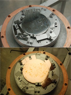
Samples of ECR-deposited thin films (top) and their substrates (copper, magnesium oxide, sapphire) (bottom). Image courtesy of Anne-Marie Valente-Feliciano.
The optimal atomic layer structures are those that minimise the so-called defect density, or the opportunity for electron scattering. Conveniently, the nature of ECR already gives scientists a head start on that front.
With ECR, no carrier gas is used – niobium ions are deposited in an environment that’s evacuated to about 2 x 10⁻⁸ torr – so there’s little chance that the system contributes impurities to the substrate. And since electric fields, rather than gases, carry the ions, they must obediently follow the perpendicular field lines that lead to the deposition site, so arriving at the metal head-on. That minimises the chances that atomic-sized voids are introduced into the layer.
But to achieve the best possible niobium layer arrangement, scientists must still contend with unavoidable atomic structural mismatches between unlike materials.
“When you grow thin films, you want to arrange them so that the substrate can be forgotten,” Valente said. The better the mismatches are masked, the more distant the reminder of aluminium or copper beneath the film, and the more closely the layers approach the behaviour of bulk niobium.
To that end, scientists at JLab have been experimenting with different substrate materials, crystallographic structures, varying temperatures and energies.
“You have to understand the correlation among radiofrequency performance, film microstructure and the method you use to produce it,” Phillips said.
Their tests have yielded encouraging results. In a series of tests with ECR-deposited niobium layers on a flat sapphire substrate, JLab researchers were able to show that they could tailor the RRR (pronounced ‘triple R’) value, a measure of the conductivity, from 10 to over 450. That wide range, said Valente-Feliciano, is testament to the technique.
Though thin films’ actual application in cavities is still some years away, JLab scientists intend to push ahead. They’re currently exploring other methods of niobium thin film deposition. They also plan to design a layer deposition system for single-cell cavities, paving the way for further experimentation with accelerator structures.
“Once you’ve reached a limit for bulk niobium, what’s next?” asks Valente-Feliciano. “Thin films are the way to the future. Now is our chance to show what they can do.”
***
Stay tuned to ILC NewsLine for more advances on thin films research. Read about another method of thin film deposition at Argonne National Laboratory.
Recent Comments