|
|||||||||||||
|
|||||||||||||
|
|||||||||||||
|
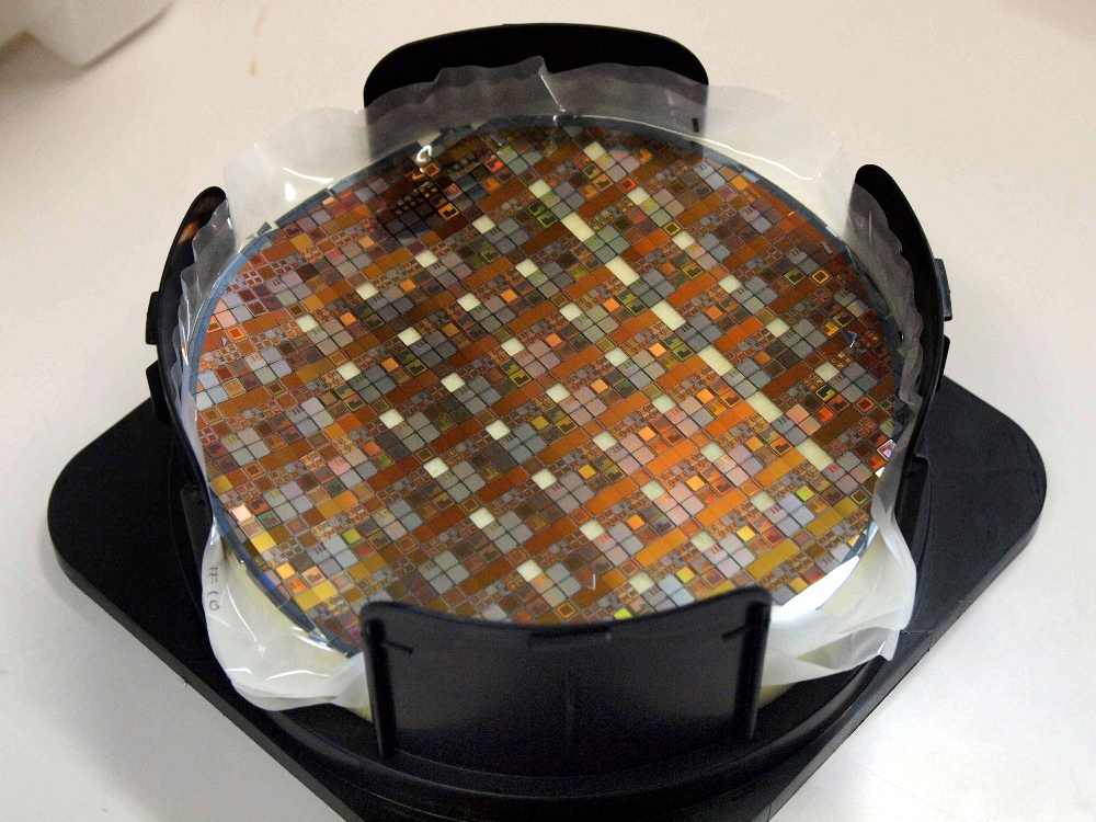
What do you visualise when you are asked about a sensor? There are many sensors around us. For example, CCDs (Charge Coupled Device), which is the basis of todays digital camera, and the technology for this year's Nobel Prize in Physics are also sensors. Thus, sensors are absolutely necessary devices for our daily life and also important technologies for the International Liner Collider. In the last years, many new sensors have been developed for the ILC, one of them being pixel sensors using Silicon-On-Insulator (SOI) technology for particle detectors, under development at KEKs Detector Technology Project Office. This sensor is expected to serve as one of the alternatives for particle sensors used in such parts as the silicon vertex detector.
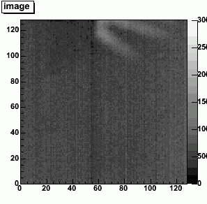
“Pixel detectors with radiation sensors and an intelligent large-scale integrated circuit on a monolithic chip have long been desired in many fields, such as high-energy physics or medical imaging,” said Yasuo Arai, a professor at KEK. “We have started the development of such a pixel detector based on the SOI technology in 2005 with the OKI semiconductor company, after KEK launched its Detector Technology Office. This new sensor's concept is very simple. We bonded two silicon wafers, low-resistivity silicon for readout electronics and high-resistivity silicon for the sensor on top of each other. The two layers are bonded with silicon dioxide, making it into a monolithic devise,” explained Arai. This SOI approach has many advantages compared to the hybrid pixel detectors, today's most advanced technologies. The hybrid pixel detectors are mainly built from two different chips: a sensor chip and a readout electronic chip bonded by a bulky metal bump. This metal bump causes problems such as multiple scattering, and limitations in pixel size or readout speed. “Applying the SOI technology, we can eliminate the metal bump, and that addresses the multiple scattering problem. It also works to reduce potential pixel size.” Moreover, SOI processes are generally tolerant to radiation, make it preferable for uses in the field such as high-energy physics, or space research. “SOI technology is not a new technology, though,” said Junji Haba, the Project Leader of Detector Technology Project at KEK. SOI technology was developed and been in practical use in semiconductor manufacturing industries from late 1990s. SOI technology has been used seeking higher speed and lower power consumption than CMOS processes in industry. “But we used it for making monolithic pixel detectors. The integrated circuits made with SOI technology have an unused silicon area. Using this area as a radiation detector, we can make monolithic pixel detectors,” said Haba. The conventional bulk CMOS process makes transistors on silicon wafers. But the SOI CMOS process makes transistors on insulators. Thus, integrated circuits fabricated on the SOI wafer have less parasitic capacity compared with conventional bulk CMOS processes, enabling higher speed and lower power consumption circuits. Currently, the new sensor is at the prototype stage. The team has developed several transistor test chips and image sensors. In the first test, they successfully fabricated the imaging sensor with 32 by 32 pixels, and confirmed the readout electronics' basic performance. Then they increased the chip size to 25 square millimetres, and number of pixels to 128 by 128, obtaining X-ray images with the prototype, the smallest size of which scaled so far is 10 by 10 micrometers. “The next step would be to improve sensor performance,” said Arai. “Our primary goal is to apply the sensor to high-energy physics and X-ray research applications.” -- Hajime Tanaka |
|||||||||||||
| © International Linear Collider |