
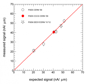
Figure 1: The signal (drain current) in response to minimum ionising particles traversing the sensor. The result is normalised to the thickness of the detector and plotted versus the expected gain. The markers correspond to different detector designs.
Solid-state devices for charged particle tracking proved their value in high energy physics in the most internal layers of the experiments of the Large Electron Positron Collider LEP at CERN, where they provided precise information on the production vertex of charged particles. These silicon micro-strip detectors consisted of a thin reverse-biased pn-junction segmented in narrow strips, each of which was read-out by an amplifier and analog-to-digital converter on a read-out ASIC. After a rapid evolution fueled by the advances in silicon technology, today these detectors are at the heart of virtually every collider experiment. In LHCb, ATLAS and CMS up to 200 square metres are equipped with these detectors. The innermost layers of the ATLAS, ALICE and CMS tracking systems, where the particle density is highest, require greater granularity than can be achieved with micro-strip detectors. The pn-junction is therefore segmented further into small rectangular pixels with sides of order 100 microns.
Despite the impressive achievements of solid-state detector R&D, the state-of-the-art devices installed in the LHC cannot meet the requirements of the experiments at a future linear electron-positron collider. To perform the precision physics that such a machine enables it is mandatory to reduce the detector material by an order of magnitude – getting it down to roughly one tenth of its original size. Several other specifications, in particular those on the spatial resolution performance, are also tighter than at the LHC. A challenge roughly comparable to that of building a car that weighs only 200 kilograms, but has greater maximum speed and the same action radius and safety of a conventional car! And there’s a catch; thin silicon sensors yield a tiny signal (80 electrons per micron) and the noise performance is degraded by the increasing capacitance to the backplane. At this point our traditional detector concept hits a solid wall and new ideas are required to make further progress.
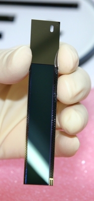
Figure 2: Photograph of mechanical sample of a thin, self-supporting DEPFET ladder
Several groups have proposed novel detector concepts that can – in principle – meet this challenge. The key to achieve the required reduction of the material is a further integration of the active material and the read-out electronics. The DEPFET concept incorporates an amplifying circuit (a “FET”) that is traditionally part of the read-out electronics in fully depleted (hence the “DEP” in DEPFET), high resistivity, detector-grade silicon, which is exactly the kind of silicon used to build conventional detectors. Thus the sensor becomes active; the tiny signal due to the ionising particle is amplified in situ. Figure 1 shows how the amplification stage in realistic DEPFET sensor prototypes allows to extract a comfortable signal – tens of nanoAmperes as opposed to 80 electrons per micron of sensor material – from extremely thin layers of silicon.
The DEPFET R&D collaboration for the Linear Collider was born at the time of the TESLA proposal (2004). A matrix of tiny DEPFET structures yields an active pixel detector that can satisfy the extremely demanding requirements on the vertex detector of a linear collider experiment. Several groups decided to join in an effort to prepare demonstrators for the TESLA experiments. Prototype sensors and Front End ASICS were designed and a mechanical concept was developed.
Results on early DEPFET prototypes were very encouraging, but unfortunately TESLA didn’t fly. By 2006 we had developed an excellent solution, but were desperately looking for a problem. Rough weather followed for LC-specific detector R&D projects. Severe budget cuts forced many promising detector concepts to look for other applications than the linear e+e– collider to ensure sufficient funding to realise a full-scale demonstrator. DEPFET found a shelter in Belle II, the detector of the upgrade project (SuperKEKB) of the B-factory at KEK in Japan. SuperKEKB was approved by the Japanese government and DEPFET was selected as the baseline technology for the vertex detector. Accepting this new challenge the collaboration received an influx of new members and has been able to ensure that the required funding for DEPFET technology reached maturity. This is not the only example of such positive side-effects of the harsh funding environment – see Marcel Demarteau’s report about spin-offs from LC-initiated detector R&D.
While the collaboration is working hard to be ready for installation of the Belle II detector in 2015, linear-collider specific activities have moved to the background. Fortunately, the experiments are quite similar and a good fraction of the new developments for Belle II are relevant also for the linear collider. Both projects share the main challenge for vertex detectors; the possibility to reduce the detector thickness to 50-75 microns makes all the difference. The emphasis on a strict control of the material budget may in fact be even more pronounced at Belle II, where most particles are very soft (hundreds of MeV) and even the thinnest sensors distort their trajectories.
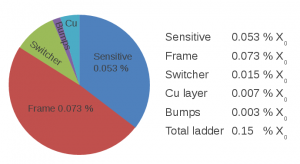
Figure 3: The material budget in radiation lengths broken down by contributions of the different ladder components for the ILC design.
A good example of the synergy between both experiments is DEPFET’s self-supporting all-silicon ladder concept, initially proposed for TESLA and adopted by Belle II. A sample image is shown in Figure 2. The material in the active area of the sensor is reduced to 75 microns. Thanks to the thicker areas around the edges the ladder has excellent mechanical properties and no external support structure is needed. The material budget for the Belle II ladder, including the silicon frame, metal layers, bump bonds and steering ASICs, is thus reduced to 0.21% of a radiation length.
A detailed finite-element simulation has been set up to predict the thermal properties of ultra-thin silicon ladders. We moreover equipped a mock-up of the Belle-II vertex detector with dummy sensors that are mechanically identical to the final sensors. The structure was used to characterise the temperature distribution of the sensors after application of a forced air flow in realistic conditions. Measurements such as those in Figure 3 have allowed for a careful validation of the finite element model. This hands-on experience has greatly increased our confidence in the viability of a cooling concept based entirely on forced gas flow.
With these new tools and the experience gained on fully engineered prototypes, it is relatively straightforward to evaluate to what extent a fully engineered DEPFET ladder meets the linear collider requirements. To stick to the previous example: we can now replace our earlier educated guesses with a much more reliable prediction of the material budget developed for Belle II. In Figure 3 the result is shown; material averaged over the ladder area in the LC design broken down by ladder components. The sum for yields 0.15 % of a radiation length. In a similar manner many other aspects of LC vertex detector performance can be extrapolated more reliably. This is – in a nutshell – the scope of our recent paper in IEEE Transactions in Nuclear Science.
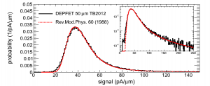
Figure 4: Signal due to perpendicularly incident charged particles. The DEPFET drain current after the integrated amplification stage is expressed in pA and normalised to the detector thickness in microns.
Perhaps the most important milestone reported in the paper is the operation of thin (50 micron) DEPFET sensors with final-design prototypes of the read-out and steering ASICs. Extrapolation of the achieved read-out speed shows that the current scheme can satisfy the ILC requirements. With this rolling shutter scheme the readout can be sped up by a factor of 2 to 4, which is adequate for ILC operation. However, single bunch time stamping at CLIC, where bunches cross twice per nanosecond, is currently impossible. A number of such read-out modules were subjected to a beam of charged pions with a momentum of 120 GeV from the CERN SPS. The signal distribution due to minimum ionising particles collected in 50 microns of silicon shows the pronounced Landau fluctuations expected from the theory for thin sensors (Figure 4). A spatial resolution is found between 1 micron, for thick DEPFETs with 20×20 mm2 pixels, and 8 micron for Belle II design sensors. A detailed model of the detector response is validated with test beam data on devices with pixel sizes between 20 and 75 microns, and then used to predict a spatial resolution of 3-4 microns for minimum ionising particles that traverse the detector under normal incidence angle, and slightly better for inclined tracks.
After the experience gained in developing a fully engineered vertex detector design we can be more confident that ultra-thin, self-supporting DEPFET active pixel detectors are a promising venue to provide precise space point measurements with a very competitive material budget. DEPFET technology is therefore a solid candidate to meet the strict requirements of the vertex detector at a future linear electron-positron collider. The installation of a DEPFET detector in Belle II in 2015 is expected to yield a demonstration of the complete detector concept.
Recent Comments